The MIMOS Technologies Sdn. Bhd. (MTSB) signed a landmark three-year Memorandum of Agreement (MoA) with Asia Pacific University of Technology & Innovation (APU) at the MIMOS Technology Preview 2026 to launch a Semiconductor Wafer Fabrication Training Programme, witnessed by MOSTI leadership, the collaboration leverages MTSB’s Semiconductor Technology Centre (STC) to provide hands-on training for APU lecturers and student cohorts, strengthening Malaysia’s semiconductor workforce pipeline.
Image
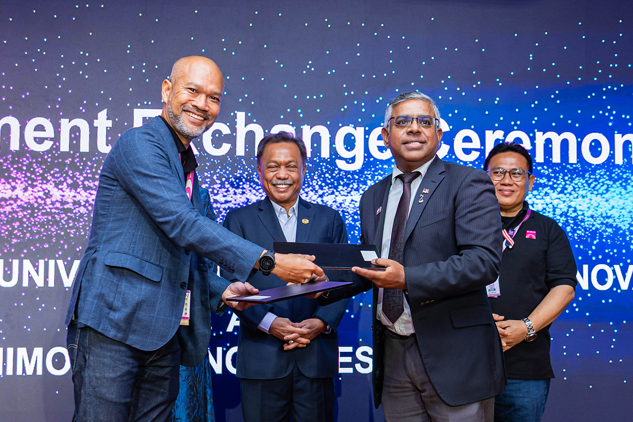
In an ambitious leap forward for Malaysia’s semiconductor landscape, the MIMOS Technologies Sdn. Bhd. (MTSB) joined forces with Asia Pacific University of Technology & Innovation (APU) to groom the next generation of integrated circuit (IC) design and chip manufacturing talents, marking APU as the first university to sign a landmark Memorandum of Agreement (MoA) with MIMOS Technologies for hands-on chip fabrication.
The two institutions formalised a landmark MoA during the flagship MIMOS Technology Preview (MTP) 2026 at MIMOS Berhad., Kuala Lumpur.
As the commercialisation arm of MIMOS Berhad. — Malaysia’s national applied research and development centre under the Ministry of Science, Technology and Innovation (MoSTI) — MTSB established this partnership to deliver an intensive, hands-on Semiconductor Wafer Fabrication Training Programme.
The agreement was signed by MTSB Chief Executive Officer, Mr Afdzal Syahadat Husni Husin alongside APU Chief Innovation, Enterprise & Sustainability Officer, Professor Ir EUR ING Dr Vinesh Thiruchelvam.
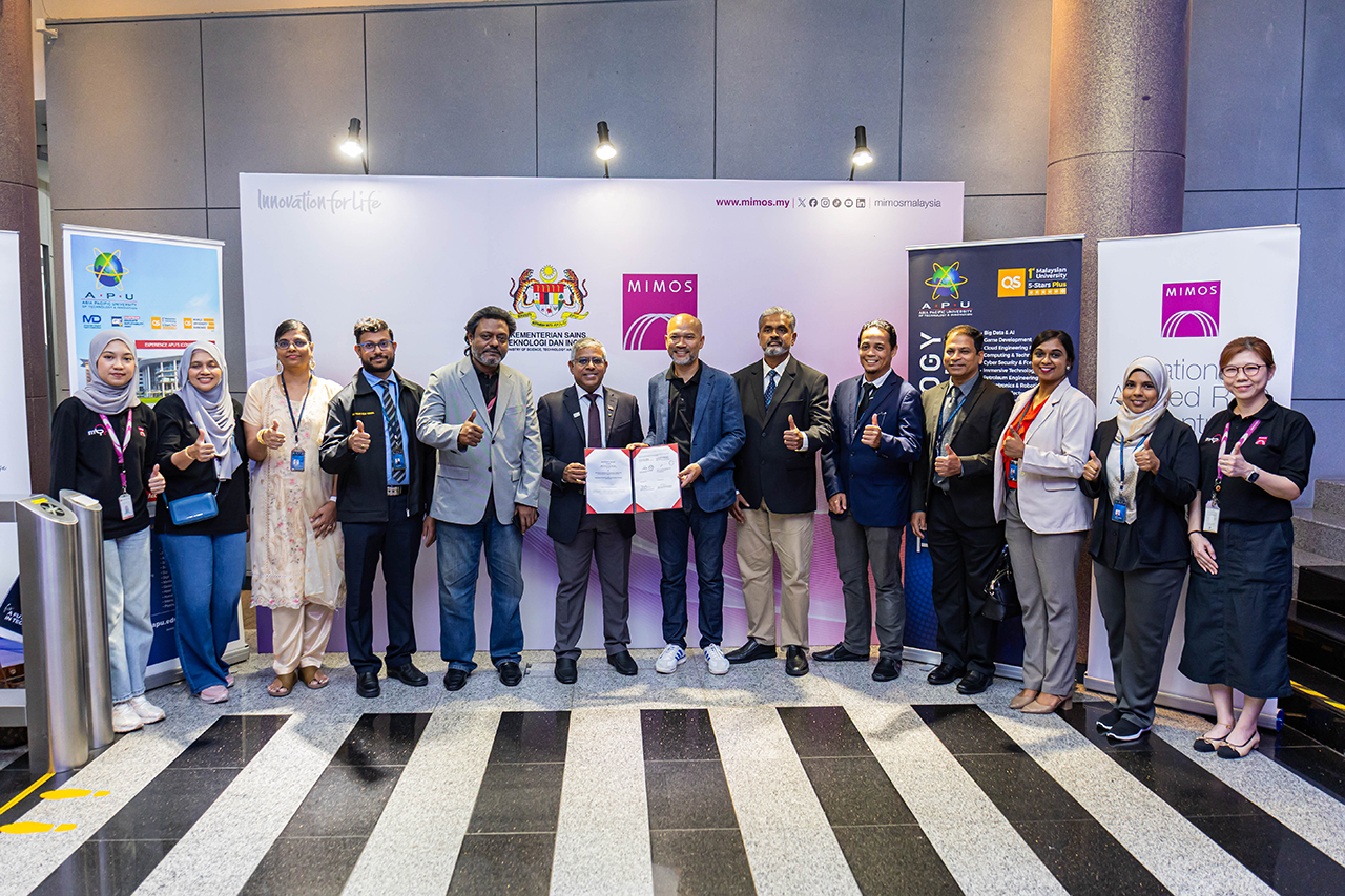
The momentous occasion was witnessed by the Deputy Minister of Science, Technology and Innovation (MoSTI), YBhg Dato’ Dr Mohammad Yusof Apdal, and President and Group Chief Executive Officer of MIMOS Berhad., Dr Saat Shukri Embong.
Also lending their presence were MTSB Chief Commercial Officer, Mr Thiagesh Kanagalingam, and APU Head of the School of Engineering (SoE), Professor Ir Dr Siva Kumar Sivanesan.
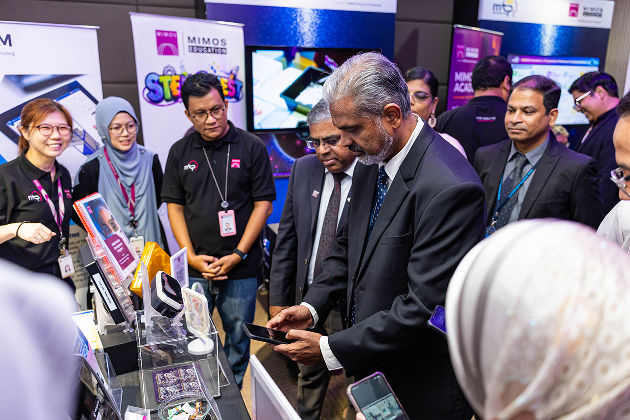
They were joined by key semiconductor lecturers from APU, including Ir Dr Mohamad Affan Mohd Noh, Assistant Professor Ts Dr Arul Paruvachi Gurusamy, Ir Ts Dr Reena Sri Selvarajan, Associate Professor Ts Dr Sathish Kumar Selva Perumal, Assistant Professor Dr Mukil Alagirisamy, Ms Noor Farhana Halil Abdul Razak, and Dr Suzana Pil Ramli.
Spanning three transformative years, the collaborative initiative directly addresses industry-academia integration, workforce readiness, and high-impact talent growth.
Under the framework, participants will gain rare, immersive access to the state-of-the-art facilities, advanced equipment, and technical expertise housed within MTSB’s elite Semiconductor Technology Centre (STC).
The strategic collaboration is structured around two specialised training pathways tailored to distinct learning profiles.
The Lecturer Training Stream offers an exclusive, one-off professional development initiative for up to seven APU engineering academics, designed to align tertiary teaching directly with cutting-edge wafer fabrication practices.
Meanwhile, the Student Training Stream will operate on a cohort basis accommodating up to 20 eligible students per intake, offering real-world fabrication room experience to bridge classroom theory and practical industry demands.
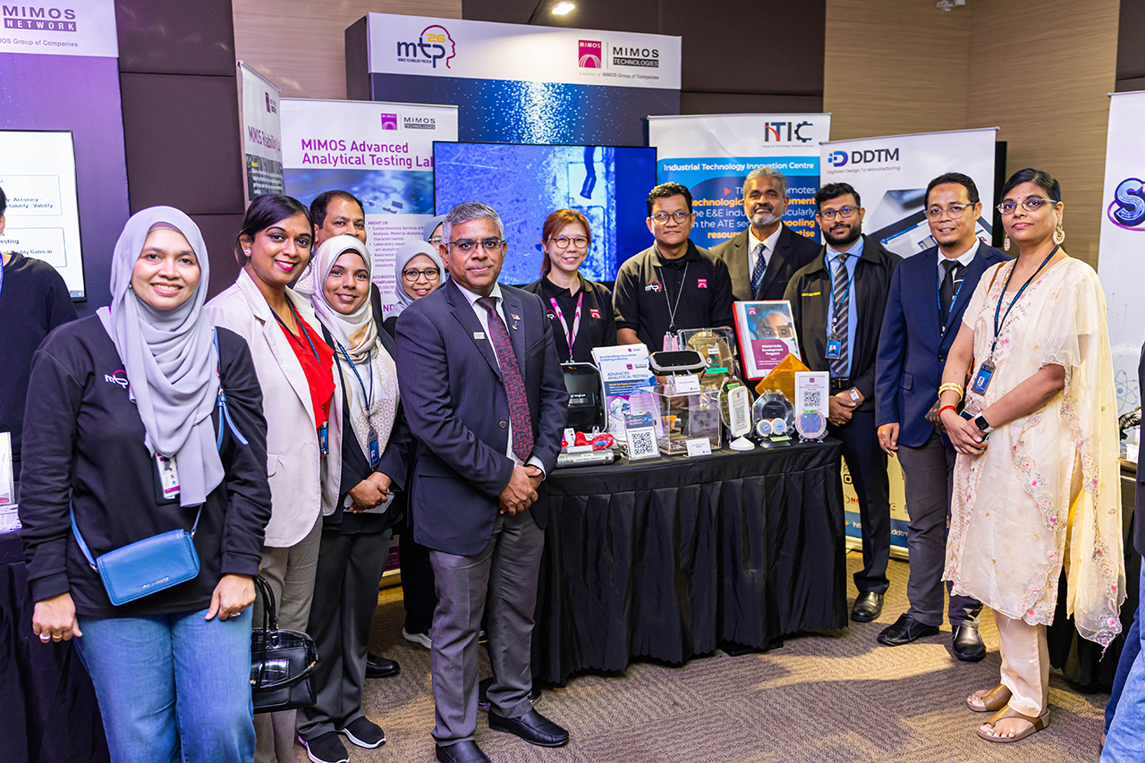
“This strategic partnership with APU marks a pivotal step in strengthening Malaysia’s semiconductor ecosystem from the ground up. By granting APU’s educators and students direct, hands-on access to the advanced capabilities within our Semiconductor Technology Centre (STC), we are bridging the gap between academic theory and high-tech industrial execution.
“At MTSB, our mission is to translate national applied research infrastructure into real-world commercial impact, and cultivating a highly skilled, industry-ready workforce in wafer fabrication is fundamental to achieving sustainable growth for our local semiconductor sector,” said Mr Afdzal Syahadat Husni Husin, Chief Executive Officer, MIMOS Technologies Sdn. Bhd. (MTSB).
Under the collaboration terms, MTSB undertakes the delivery of custom technical modules, standard safety protocols, and direct mentorship by qualified industry specialists at the STC.
Simultaneously, APU will oversee participant selection, administrative coordination, and strict compliance with operational and intellectual property safeguards.
“Signing this landmark agreement as the first university partner with MIMOS Technologies underscores APU’s ongoing commitment to industry-centric education and high-impact talent creation.
“Access to state-of-the-art chip fabrication facilities allows our faculty to stay at the cutting edge of semiconductor developments while offering our students an invaluable, real-world experience inside an advanced cleanroom environment.
“Through targeted pathways for both our academic staff and student cohorts, we are empowering our engineers to enter the market with the practical mastery required to drive Southeast Asia’s semiconductor innovation forward,” said Professor Ir EUR ING Dr Vinesh Thiruchelvam, APU Chief Innovation, Enterprise & Sustainability Officer.
By uniting academic excellence with national research infrastructure, APU’s School of Engineering (SoE) continues to solidify its reputation as a premier launchpad for high-value semiconductor engineering talent in Southeast Asia.
News & Happening
Download e-Brochures
Intake Calendar
Want to know more ?
Let’s Connect