APU Students Gain First-Hand Insights at MIMOS
On 7th August 2025, a group of 43 engineering students from the Asia Pacific University of Technology & Innovation (APU) embarked on an industrial visit that would leave a lasting mark on their educational journey.
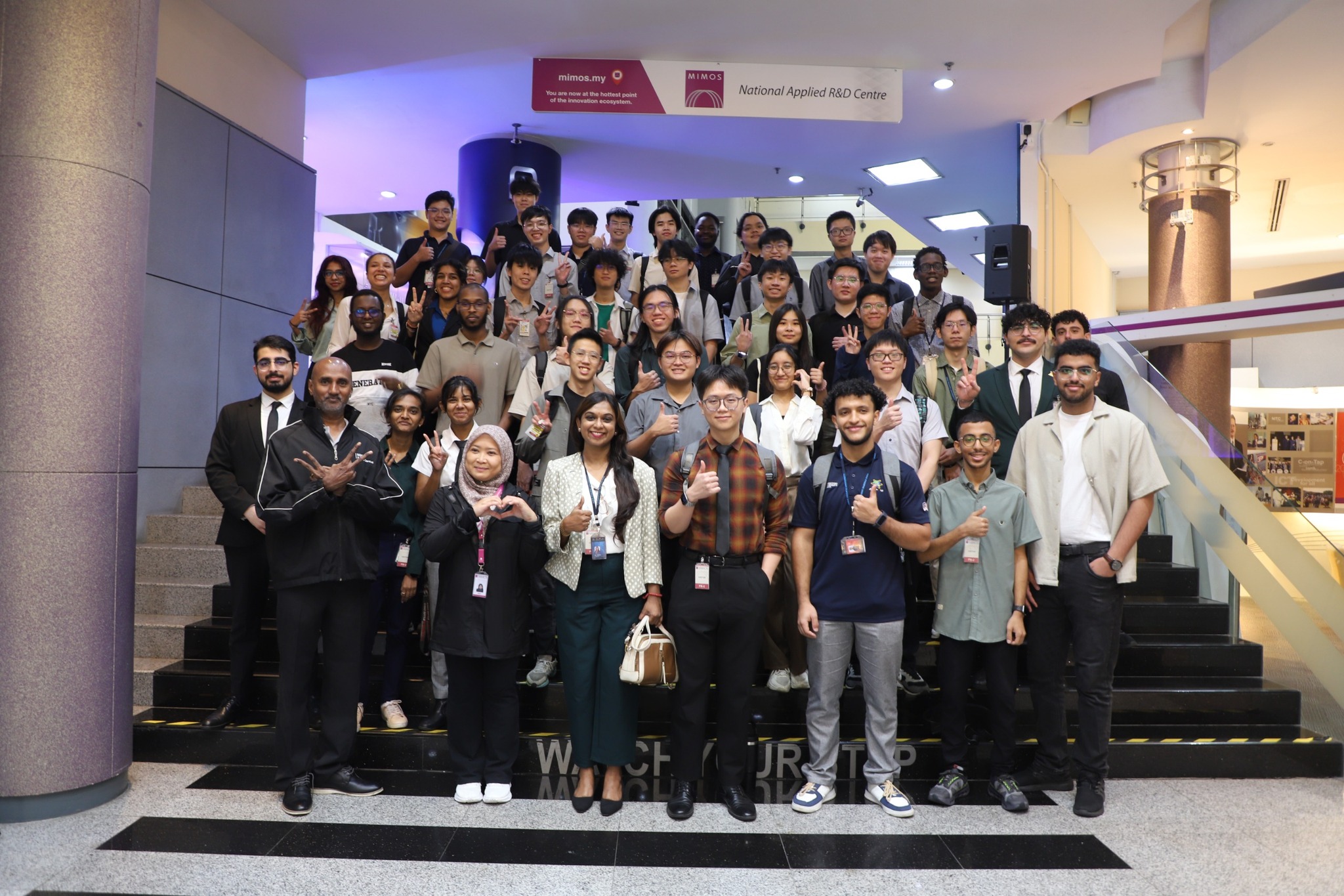
Hosted by MIMOS Berhad, Malaysia’s National Applied Research and Development Centre under the Ministry of Science, Technology and Innovation (MOSTI), the visit offered a rare glimpse into the nation’s cutting-edge research in microfabrication and failure analysis within the semiconductor and IC chip-making industry.
This initiative reflects APU’s long-standing strength in creating opportunities for its students to bridge classroom knowledge with real-world applications. Right before they step into professional careers, APU engineers are trained not just to understand theory, but immerse themselves in hands-on learning experiences like this.
A Journey Led by Expertise
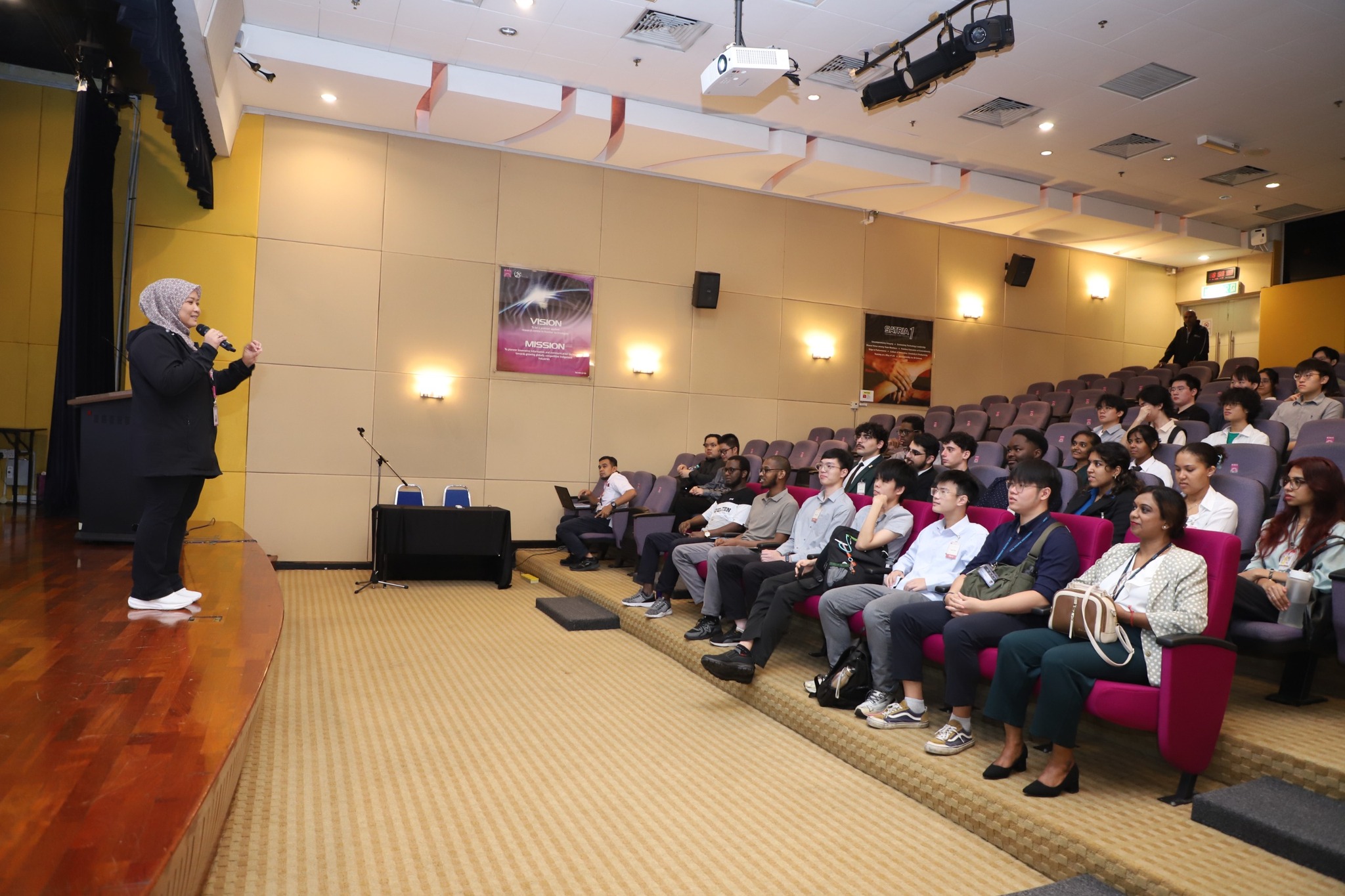
The visit was led by Ir Ts Dr Reena Sri Selvarajan, Senior Lecturer at APU’s School of Engineering (SoE). For Dr Reena, the visit was especially meaningful as her own research journey began in a field closely aligned with MIMOS’ advanced work.
“Seeing these sophisticated facilities in action has inspired my students to think beyond textbooks to imagine themselves as innovators contributing to Malaysia’s growing high-tech industry,” she shared.
Learning the Art and Science of Engineering
The half-day programme unfolded in two carefully designed sessions: an interactive talk followed by a guided lab tour.
To set the tone, Mr Wan Mohd Tasyrif Wan Yaakob, a Failure Analysis Engineer at MIMOS, delivered a talk that captivated the audience. He revealed the meticulous processes engineers employ to detect faults in electronic components—an invisible yet crucial discipline.
Using real-life examples and state-of-the-art tools, Mr Wan demonstrated how tiny imperfections could make or break a device’s performance, highlighting the pivotal role engineers play in solving these high-stakes challenges.
Immersed in the Lab Experience
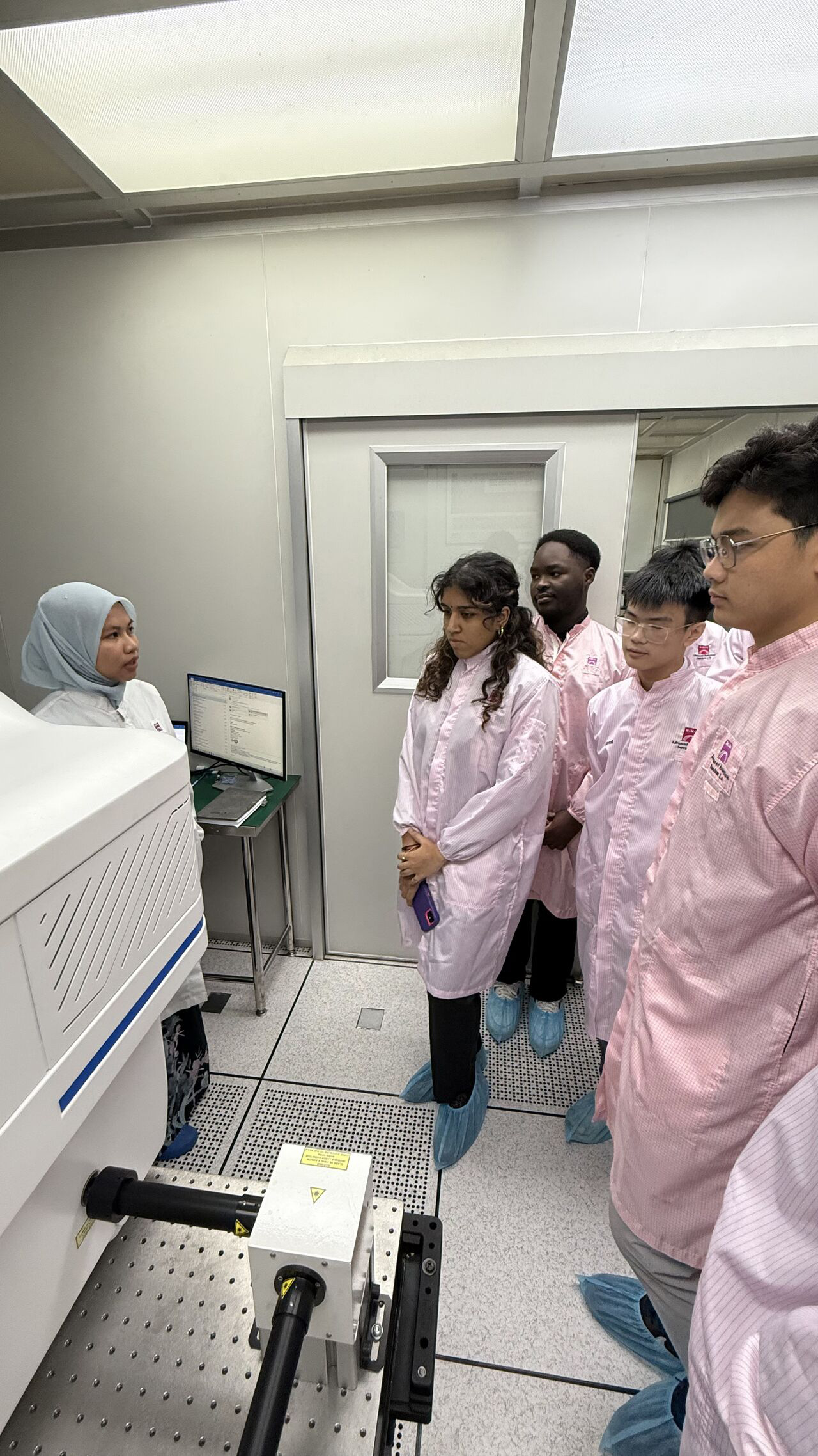
The highlight of the day came when students stepped into MIMOS’ world-class laboratories. Before entering, they suited up in cleanroom gowns, experiencing first-hand the strict protocols of working in a high-precision environment. For many, this was a transformative moment—slipping into the shoes of a microfabrication engineer.
Inside the Nano Lab, students witnessed the fascinating process of photolithography, where silicon wafers are turned into the tiny integrated circuits (ICs) powering everyday devices, from smartphones to computers.
Watching the chip-making process unfold step-by-step, APU students gained a newfound appreciation for the complexity behind modern technologies.
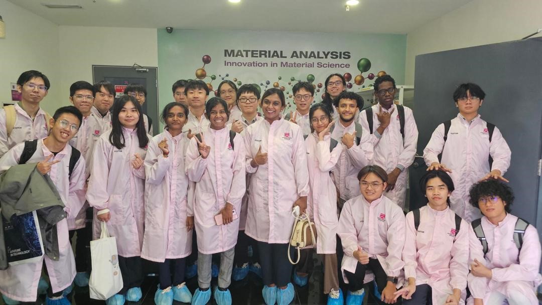
The journey continued into the Failure and Material Analysis Lab, where towering multi-million-ringgit machines stood ready to expose microscopic defects invisible to the naked eye.
Guided by expert technicians, students asked questions, explored advanced instruments, and saw firsthand how cutting-edge science is applied in solving real engineering challenges.
A Glimpse into Tomorrow
For APU students, the visit was more than just an academic exercise—it was a chance to imagine their own futures. Each lab, each conversation with MIMOS engineers, offered not just knowledge but inspiration.
They left not only with answers but with new questions, eager to explore where their engineering journey might take them.
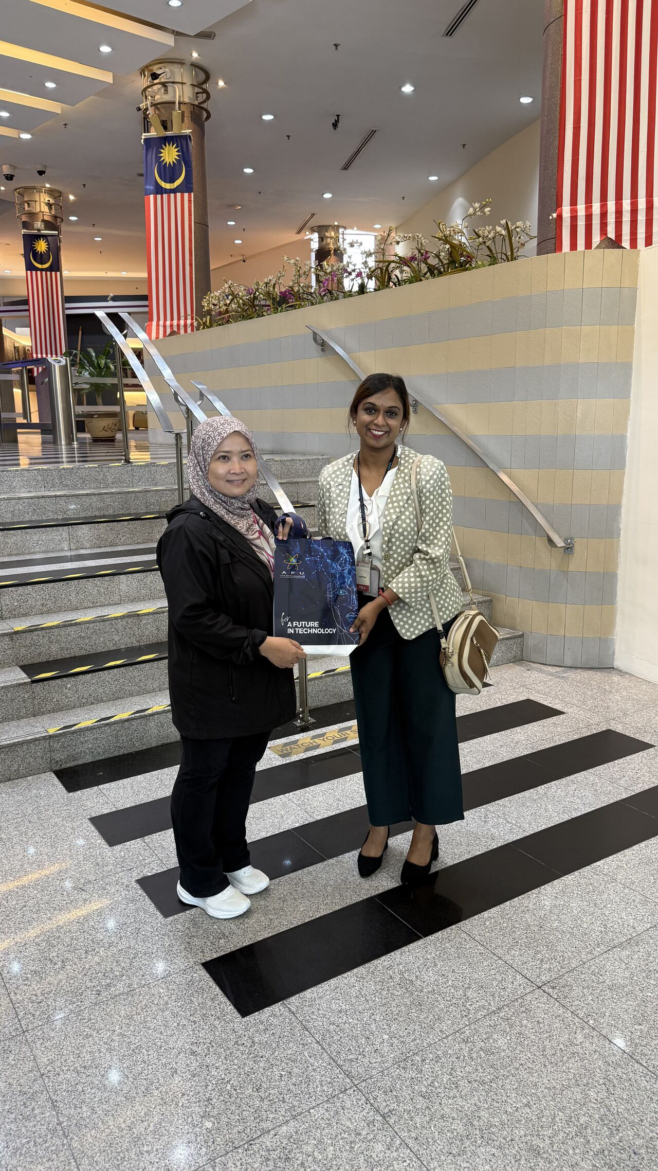
The day concluded with a group photo and a token of appreciation presented by Dr Reena to the MIMOS team. For the students, however, the most valuable takeaway was intangible: the vision of themselves as future contributors to Malaysia’s high-tech landscape, ready to carry forward the spirit of innovation.
News & Happening
Download e-Brochures
Intake Calendar
Want to know more ?
Let’s Connect